


Samsung Electronics Executive Chairman Lee Jae-yong toured the company's chip facilities in Gyeonggi Province, emphasizing the recent improvement in chip production performance of its Device Solutions (DS) Division.
The company stated that Lee toured the NRD-K construction site, a 109,000-square-meter R&D complex that Samsung is developing in the Giheung District of Yongin, Gyeonggi Province, with a planned investment of 20 trillion won ($13.5 billion) by 2030.
Also Read: Japanese Semiconductor Industry's Profits Reflect Demand for AI
NRD-K started setting up its facilities in November of the previous year, incorporating high-resolution extreme ultraviolet lithography machinery for developing next-generation memory semiconductors, deposition equipment for new materials, and wafer bonding infrastructure intended to facilitate the joining of two wafers.
During the visit, Lee received updates on the latest advancements in next-generation technologies for memory, foundry, and system semiconductors, and examined new R&D facilities set up in the cluster.
He additionally toured the division's Hwaseong Campus in Gyeonggi Province, where he examined manufacturing automation systems driven by digital twin technology and robots, along with the implementation of AI technologies throughout campus operations.
Also Read: Netmarble Chairman Spearheads Social Value Initiatives
During the site visit, Lee met with Jun Young-hyun, Vice Chairman of Samsung Electronics and head of the DS Division, along with DS Division Chief Technology Officer Song Jai-hyuk and other executives to discuss recent advancements in the semiconductor sector.
During the visit, Lee urged the firm to “reestablish essential technological competitiveness through daring innovation and investment,” as stated by Samsung Electronics.
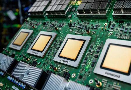
He additionally conducted a distinct meeting with staff in development, manufacturing, and quality control, paying attention to input from frontline employees who played a role in the commercialization of advanced semiconductor products, such as high-bandwidth memory (HBM), D1c DRAM, and V10 NAND flash memory.
Lee’s visit is viewed as a way to motivate the division’s employees and researchers, who displayed significant enhancements in performance during the latter half of this year.
Also Read: FTC Chief Says to Narrow Differences in Platform Regulations
In the initial quarter of the year, Samsung Electronics relinquished its top position in the global DRAM sector to competitor SK hynix, as its HBM chips for AI accelerators were surpassed.